


Advanced Pad Features

Advanced pad features accurately model the electrical effects of component mounting pads, including parasitic capacitance and discontinuities introduced by PCB layouts. By accounting for these real-world influences, designers can achieve more realistic circuit simulations, improved agreement between simulated and measured results, and greater confidence in first-pass design success.

Modelithics models include additional Advance Pad Features, in many models within the Modelithics COMPLETE Library™, including such features as: Pad Angle, Pad in Model, Solder Mask and Solder Paste. See below for additional details regarding each feature.

Pad Angle

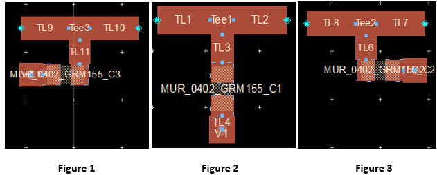
“Pad Angle” changes how the pads are connected in the layout and alters the model response accordingly. There are two PadAngle parameters in each model, so that the pad connection angle can be set for each pad independently. That is, the PadAngle1 parameter affects the pad at port 1 and PadAngle2 affects the pad at port 2. Pad Angle changes the direction at which the adjacent component connects with the model pad. The available options are:

  •  0 Degrees (Default) – Pin at the outside edge of pad along the width. See Figure 2.
  •  -90 Degrees – Rotates the pin clockwise. See Figure 1.
  • Degrees – Rotates the pin counter-clockwise. See Figure 3.
Pad in Model

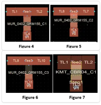
Pad In Model is another feature that was added with the v17.x release and can be applied to each pad separately. The PadInModel parameters alter the percentage of the pad calculated by the model and change the location of the pin. Valid values for Pad In Model are:

  • 100%: reference plane at edge of pad (Default). See Figure 4.
  • 50%: reference plane at center of pad. See Figure 5.
  • 0%: reference plane at edge of part. See Figure 6.
  • Shunt: part mounted on microstrip line. See Figure 7.
Solder Mask

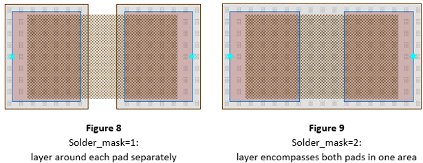
The Solder Mask parameter as well as the associated Solder Paste parameter were added in response to customer requests. The Solder Mask parameter has three settings:

  • 0: No Solder Mask.
  • 1: Pads Separately. See Figure 8.
  • 2: Pads Together. See Figure 9.


The default value “No Solder Mask” does not draw a solder mask in the layout. The “Pads Separately” option draws a box around each of the pads in the layout. Use the MaskAperture parameter to define the size of the solder mask opening around both pads. The default value of the aperture is 75um.

Solder Paste

Like Solder Mask, this feature only affects the model layout. Neither feature changes the model’s simulation response. The Solder Paste feature has 2 settings

  • 0: No Solder Paste.
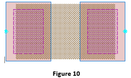
  • 1: Include Solder Paste See Figure 10.

As with Solder Mask, the Solder Paste default is to not draw the solder paste layer and is set to “No Solder Paste”. When the parameter is set to “Include Solder Paste” an additional layer with specified aperture is created in the layout, using the “Paste Aperture” parameter value to determine the size of the aperture relative to the pad. As with the Mask Aperture setting, this value can be either positive or negative which determines if the aperture circumscribes or inscribes the pads respectively. The default value for this parameter is -75um.

Design Faster With Measurement-Based Models

Access accurate, measurement-based models and services built for reliable RF and microwave simulation.

Modelithics Vendor Partners

Request a Model

Our new website is live

Welcome to Our New Website!

We’re excited to introduce our newly redesigned website, featuring improved navigation, enhanced resources, and a better overall experience. Explore the new site and discover what’s new.