When designing high frequency circuits, parasitic effects can drastically deteriorate circuit performance if not appropriately addressed. It is not enough to simply run a schematic level simulation even if including transmission line interconnect effects. The best chance a designer has at first-pass design success is through incorporating high-accuracy parasitics models for all lumped elements or active devices in a design, combined with accurate electromagnetic analysis for any passive interconnect structure. As outlined in various resources, the methods for combining electromagnetic analysis and lumped parasitic models is not always straightforward and can be somewhat involved [1]-[6].
The purpose of this paper is to describe a recommended procedure for using Microwave Global Models™, as included in Modelithics® CLR Library, in conjunction with NI/AWR’s AXIEM® 3D planar electromagnetic analysis tool. To illustrate this process, EM co-simulation is compared to measured S-Parameter data of an elliptic high-pass filter.
Nuhertz Technologies’ FilterSolutions® software was used to generate the high-pass elliptical filter design featured in this paper. The design process starts by establishing and entering design requirements into the FilterSolutions software and interactively using Modelithics CLR Library models along with NI/AWR Microwave Design Environment in a procedure similar to that described in reference [7]. The design goals for this filter are: 5GHz center frequency, maximum passband ripple of 0.05dB, stopband ratio of 1.2 and stop band attenuation of 25.27dB.
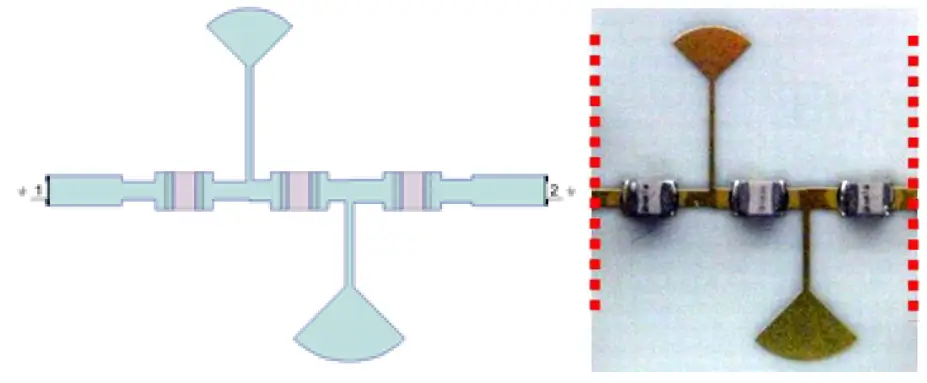
The design process proceeds by selecting the filter topology (elliptical high-pass) and other design options such as frequency, rejection and bandwidth requirements. The result of the synthesis that follows is a hybrid lumped / distributed element filter design based on ideal components. A substrate material (20mil Rogers 4003C) and the Modelithics model part family (CAP-ATC-100A-001) are then selected and substituted into the ideal filter design. The design schematic diagram and layout are exported from FilterSolutions to NI/AWR Design Environment for optimization and further analysis (Figure 1). As explored later in this paper, the inclusion of Modelithics accurate parasitic models aids prediction of, and facilitates compensation for, the impact of parasitic effects.
After inclusion of the parasitic models, the most dramatic changes in response are, shifting of the entire pass-band to a lower frequency range and degradation of the out-of-band rejection. In order to compensate for these changes, the schematic diagram must be optimized. The first optimization is completed on the component part values. This optimization will determine the correct component values needed to compensate for the frequency shift caused by the internal parasitics of the SMD components and the substrate. After the first optimization is complete, FilterSolutions will select the closest part value from the Modelithics model part family defined earlier. The second optimization is performed on the interconnect line lengths and widths to further improve performance. More information on this process can be found in [7].
FilterSolutions automatically sets up an EM analysis; however the EM structure itself as well as port configurations must be modified to obtain the most accurate results. The EM analysis setup procedure for Axiem is the focus herein. This straightforward design process helps to eliminate guesswork and greatly simplify and speed-up what is normally an extremely iterative and manually intensive filter design flow.
Figure 1. Left – Layout of 5GHz elliptic high-pass filter. Right – Fabricated 5 GHz elliptic high-pass filter on 20mil Rogers 4003C. Dashed red lines indicate measurement reference planes.
Simulating Pad Stack Effects
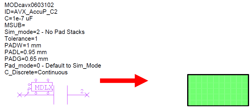
By default, Modelithics models include both substrate and solder pad (“pad stack”) effects. There are two ways to complete co-simulations with Modelithics models: 1) allow the model to account for all parasitics including pad stack effects (Sim_mode=0) and omit pad geometries from the EM simulation, or 2) remove the pad stack effects from the parasitic model (Sim_mode=2) and include pad geometries in the EM simulation. As long as the pads used fall within the Modelithics model’s valid pad range, either method will produce similar results. The advantage of performing an EM simulation with the pad geometries included is the inclusion of step discontinuity effects when the pads are a different width than the feed line. (For more information on using the Sim_mode parameter, see Modelithics Application Note 37 [2]).
EM Extraction Setup
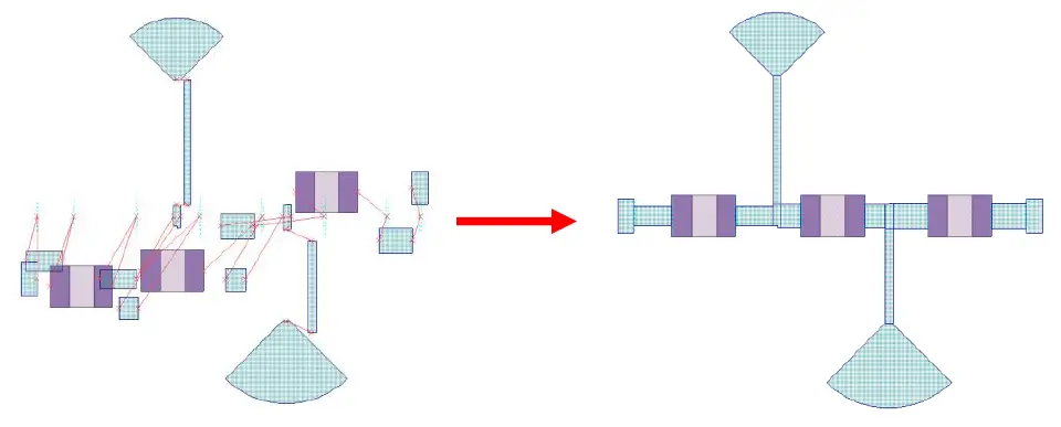
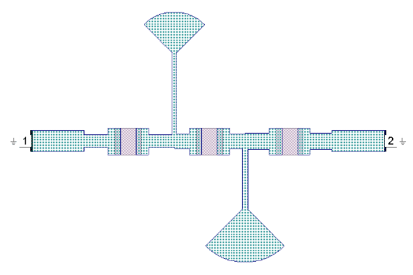
The designer may decide to draw their layout from scratch in AXIEM or, if a schematic with transmission line elements exists, the designer may choose EM extraction. This app note will focus on extracting the EM structure from a previously created schematic. To extract an EM Structure from a schematic, view the schematic layout and ensure the layout is correctly snapped together. If not, select all elements in the layout and go to Edit Menu > Snap Together (Figure 2). Failure to snap together the layout prior to EM extraction can cause errors.
Figure 2: Incorrect layout (left). Layout correctly snapped together (right).
NI/AWR Design Environment contains a script to generate automatically the EXTRACT and SUBSTACK elements to be used in Axiem. To use this utility, all the designer must do is set the schematic containing the MSUB element as the active window and go to Scripts > EM > Create_stackup, review the substrate and grid size, and check the “Union Shapes” and “Explicit Ground (Lower)” options in the EM Extraction dialog window. (For more information on AXIEM substrate setup see reference [3]). Review the schematic and ensure all transmission line elements are enabled in the EM extraction. This is completed by double-clicking the model and ensuring the “enable” box is checked under Properties > Model Options > EM Extraction. Once setup is complete, right-click the EXTRACT block in the schematic and select Add Extraction to create the EM document. The resulting EM structure will contain all elements enabled for EM Extraction.
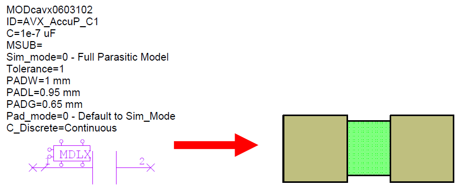
The following section describes a procedure for including pads within the Axiem simulation and modifying the EM structure to correctly set the reference planes for Modelithics models in Sim_mode=2 (Figure 4). For simplicity, if the pad stack is excluded from the Axiem simulation and the Modelithics models are in Sim_mode=0 (Figure 3), skip directly to the “Port Configuration and De-embedding” section.
Modifying EM the Structure for simulation using Sim_Mode=2
In this section, the pad stack effects are excluded from the Modelithics models and simulated within the AXIEM simulation. Removing the pad stack effects from the Modelithics model is accomplished by setting the model’s Sim_mode parameter to 2. Newer versions of the Modelithics CLR library have an additional parameter that influences how the pad stacks are treated. The Pad_mode parameter must be set to 1 to include the pads in the layout1. Doubleclick on each model and verify the “enable” box is checked under Properties > Model Options > EM Extraction. Once the setup is complete, right-click the EXTRACT block in the schematic and select Add Extraction to create the EM document. The resulting EM structure will contain all transmission lines and pads, as well as also blocks representing the physical components’ position on the pads. The next step is to setup the correct reference planes for the ports.
Figure 3: Example of Modelithics model with Sim_mode=0 in schematic view (left) and layout view (right).
Figure 4: Example of Modelithics model with Sim_mode=2 in schematic view (left) and layout view (right).
Start with the newly extracted EM Document (Figure 5). All transmission line elements, should already have had the Union operation performed. Change the material for all pads to match that of the transmission lines and perform another Union operation.
Figure 5: Newly extracted EM Document.
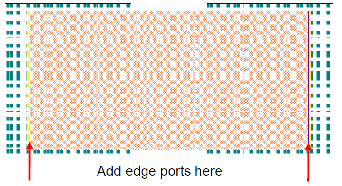
In the cases studied, the best results were obtained using edge ports. By default, Axiem will not allow an edge port to be defined in the middle of a conductor. Normally, this would imply that it is not possible to perform a simulation with the model reference planes defined mid-pad as would be needed for Sim_mode=2. However, by adding a thin strip of conductor (made of the same material as the rest of the transmission lines in the circuit) at the location of the part edge on the pad, it is possible to define an edge port at the correct location.
Proper placement of the conductor strip is shown in Figure 6. Now add edge ports to the conductor strips on the common edge between conductor strip and component. Once all edge ports have been defined, delete the block representing the component (maroon rectangle in Figure 6) from the EM structure.
Figure 6:. Illustration of component (maroon) sitting on pads (green). The proper positioning of the additional conductor strip is shown in yellow.
Port Configuration and De-embedding
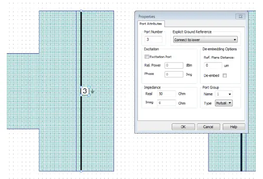
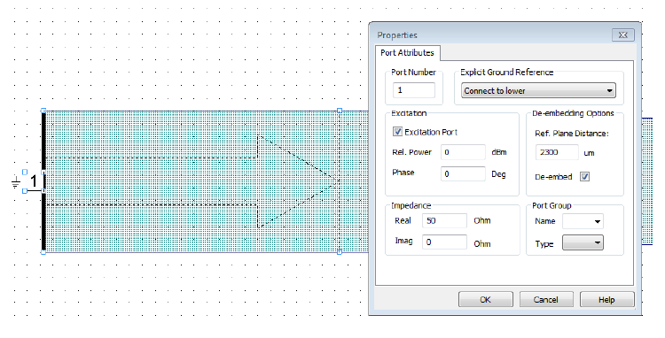
The appropriate port configuration that will give the most accurate results depends on the spacing of the layout. If the edge ports are at least two times the substrate height removed from any metal (other than the line to which they are connected), the ports should have the Explicit Ground Reference parameter set to “connect to the lower.” The De-embed option should be enabled and Ref. plane distance set to zero. However, better results will be obtained by setting the Explicit Ground Reference to “none” and disabling de-embedding, if the spacing constraint is not met. For more information on de-embedding in AXIEM, see references [4] and [5]. To remove coupling between neighboring ports, go to the Port Groups section and assign a unique name for each port pair, set the type to “mutual.” This is done since Modelithics models already account for pad-to-pad coupling.
Figure 7: Port setup to connect Modelithics models.
For the input and output ports, draw a conductor box the same width as the line. Make the line length twice as long as the line width or twice the substrate height, whichever is larger. Add an edge port, set Explicit Ground Reference to “connect to the lower,” enable de-embedding, and set the Ref. plane distance equal to the additional line length.
Figure 8: Port setup for input and output ports.
Note on Using Metal Thickness
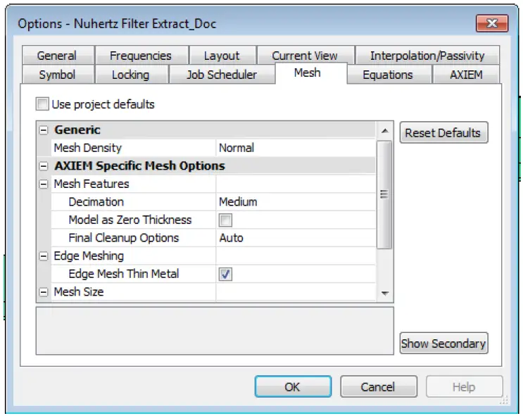
With some layouts, allowing AXIEM to simulate the EM structure as a planar object (zero thickness) will yield satisfactory results. However, when the gaps between lines in the layout are on the order of the line widths used, this simplification may no longer produce accurate results and the layout will need to be simulated as a 3D object. AXIEM can be set to use the line thickness specified in the Enclosure Settings by right clicking the EM structure and entering the Options dialog. In the Mesh tab, uncheck the “Model as Zero Thickness” box.
Figure 9: Enclosure Options dialog..
Meshing in AXIEM
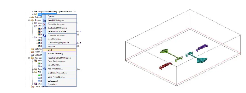
Now, mesh the EM structure by right-clicking the EM structure and selecting Mesh. Check the mesh to make sure the port setup is correct and the mesh is not producing errors in the Status Window. An example of a common error/warning when meshing an object is the “high aspect ratio facets” message. When AXIEM creates a mesh, each area is called a facet. The aspect ratio of a facet is the ratio of its width to its height. A warning is given but simulation proceeds when the aspect ratio of a facet exceeds 100; however, an aspect ratio exceeding 1000 results in an error and failure of the simulation.
Common causes of high aspect ratio facets is shape misalignment and using curved structures without directing AXIEM to simplify the structure. To simplify the structure, enable “Decimation” under the Mesh tab. Adding a HI_ASPECT_FACETS annotation to the EM document will allow viewing of the problem areas and corrections to the layout. High aspect ratio facets are a sign that the mesh is not appropriate to solve the problem. They unnecessarily increase the number of facets, and can also cause numerical instabilities when solving the EM structure.
Figure 10: Example of meshed EM structure. Note that all ports are grounded.
Simulation and Results
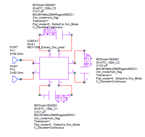
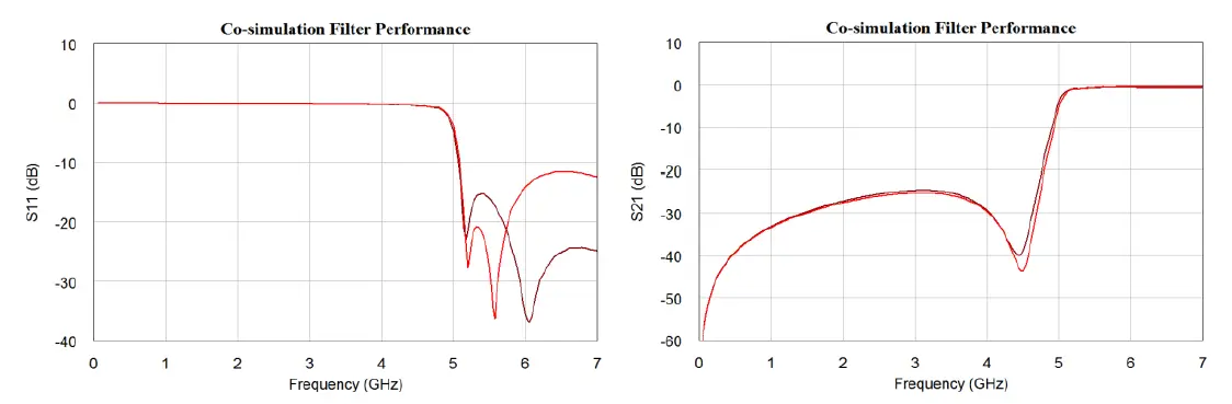
Now disable the EM extract block in the schematic. Leaving the EM extract block active will overwrite all modifications made to the EM Document. Right-click the EM Structure and select Simulate. Once the EM data has been generated, create a new schematic including a subcircuit element and connect the Modelithics models across the appropriate ports (Figure 11). Simulate this schematic to obtain the results of the co-simulation. The final filter response comparing the effect of Sim_modes in the EM co-simulation can be seen in Figure 12.
Figure 11: Schematic used for co-simulation.
Figure 12: Comparison of EM co-simulation with pads included (red line) versus EM co-simulation without pads (brown line).
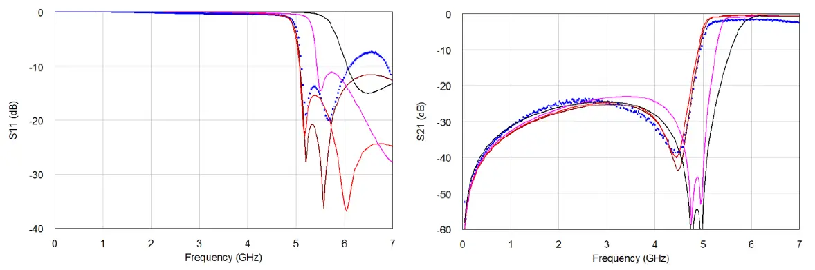
To validate the results of the EM co-simulation results, the 5GHz elliptic high-pass filter was fabricated and tested on a 20mil Rogers 4003C substrate. Figure 13 shows the progressive improvement in simulation to measurement agreement as more parasitic effects are included. Not surprisingly, the ideal circuit simulation (black) shows poor agreement with measured data. The parasitic simulation including substrate effects and component parasitic effects (magenta) shows improvement over the ideal simulation, but the cut-off frequency is still not accurately predicted. This is likely because the filter is a hybrid lumped element / distributed filter. Although the inclusion of Modelithics models accurately captures the capacitor performance, interactions of the layout and the radial stub transmission line model may not be fully captured with only the circuit-level simulation. This is why the use of EM co-simulation (red and brown) results in a more accurate prediction of cut-off frequency, pass-band behavior, and more closely models out-of-band performance.
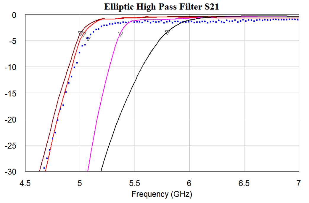
Figure 14 shows a narrowband comparison of 3dB cut-off frequency prediction by simulation versus measured data. Table 1 lists the 3dB cut-off frequencies of all simulations and shows the calculated percent error of the predicted cut-off frequency from the measured cut-off frequency. The cut-off frequency of the high-pass filter was predicted accurately by EM co-simulation within 0.8% of the measurement. This is a drastic improvement over the 14.3% shift in cut-off frequency prediction by the ideal circuit-level simulation. Failing to account for parasitic, substrate, and layout effects when designing this high frequency circuit would have caused a severe discrepancy between design goals and realized filter performance. However, using accurate parasitic models to account for the parasitics of the components combined with EM analysis to account for layout effects, first-pass design success was achieved with this filter design.
Figure 13: S11 (left) and S21 (right) for an elliptic high pass filter. Black line – circuit simulation results using ideal components without EM co-simulation Magenta line – circuit simulation results using Modelithics models without EM co-simulation Red line – EM co-simulation using Modelithics models (Sim_mode=2) including pads in layout Brown line – EM co-simulation results using Modelithics models (Sim_mode=0) excluding pads from layout Blue symbols – measured S-Parameter data
Table 1: 3dB cut-off frequencies for simulations and measured data. Percent error for simulated 3dB cut-off frequency versus measured 3dB frequency.
Conclusion
When using Modelithics models with AXIEM, it is recommended to use explicitly grounded, deembedded edge ports when the ports are separated by at least two substrate heights. Mutually grouping these port pairs removes the coupling between pads already accounted for in the Modelithics models. If the layout does not permit two substrate heights of separation between placement of edge ports, better results can be obtained by using implicit grounding and disabling de-embedding. This application note demonstrates a procedure to improve simulation to measurement agreement using Modelithics models in conjunction with AXIEM EM simulation.
Figure 14: Narrowband view of high-pass filter S21 response showing the accuracy of the 3dB cut-off frequency predicted by each simulation versus measured data.
Black line –simulation results using ideal components without EM co-simulation Magenta line – circuit simulation results using Modelithics models without EM co-simulation Red line – EM co-simulation using Modelithics models (Sim_mode=2) including pads in layout Brown line – EM co-simulation results using Modelithics models (Sim_mode=0) excluding pads from layout Blue symbols – measured S-Parameter data.
References
[1] “A Plethora of Ports: Making Sense of the Different Types of Ports in AXIEM,” Application Note, National Instruments AWR, n.d. Web. .
[3] “Using the Electromagnetic Simulator,” AWRDE Getting Started Guide: Chapter 7. MWO, National Instruments AWR, n.d. Web. .ensitivity Analysis,” Modelithics – Literature, Modelithics, Inc., 02 Nov. 2012, Web. www.modelithics.com
[4] J. Dunn “EM Tips and Tricks for the Circuit Designer,” IEEE Microwave Theory and Techniques Society Monthly Meeting, Japan House, Dallas, Texas, 29 Mar. 2011, IEEE Microwave Theory and Techniques Society Dallas Chapter, Web. . J. Dunn “Ten Things Every Designer Should Know When Using AXIEM,” AXIEM™ Best – Practice Guide, National Instruments AWR, n.d. Web. .
[5] S. Skidmore, J. Boh. “APPLICATION NOTE 048: Recommendations for Port Setup When Using ADS Momentum and Modelithics Models,” Modelithics – Literature. Modelithics, Inc., 11 Aug. 2014. Web. .
[6] I. Delgado, L. Levesque, L. Dunleavy and J. Kahler, “Synthesize Filters with Wideband Success,” Microwaves & RF , July 2014.
[7] I. Delgado, “APPLICATION NOTE 052: A Design Flow for Rapid and Accurate Filter Prototyping,” Modelithics – Literature. Modelithics, Inc., 30 June 2015. Web. .
About this note
This note was authored by Isabella Delgado (student intern at Modelithics) with substantial help from Scott Skidmore (Modelithics), Scott Muir (student intern at Modelithics, now with Qorvo) and Mark Saffian (AWR Group, NI).
Contact Information
For more information about Modelithics’ products and services, please contact Modelithics, Inc., Email: sales@modelithics.com / Web : www.modelithics.com
All other trademarks are property of their respective holder.